
Electronics / Semiconductor
Electronic parts demand accurate marks with damage-free results. Learn how KEYENCE lasers accomplish both.
Electronic Components: Direct Part Marking
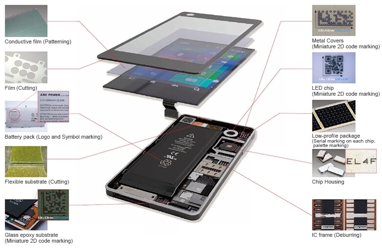
Personal electronic devices, such as smartphones and tablets, have seen a rapid increase in sales in recent years. At the same time, the number of components and miniaturization of components inside these devices is accelerating.
Manufacturers must thoroughly implement traceability control to ensure high quality products. The miniaturization of components has prompted many manufacturers to replace conventional machining with laser machining. Lasers markers are contactless and more accurate than traditional devices, making them ideal for marking electronic components.

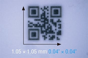
Case1.2D code marking
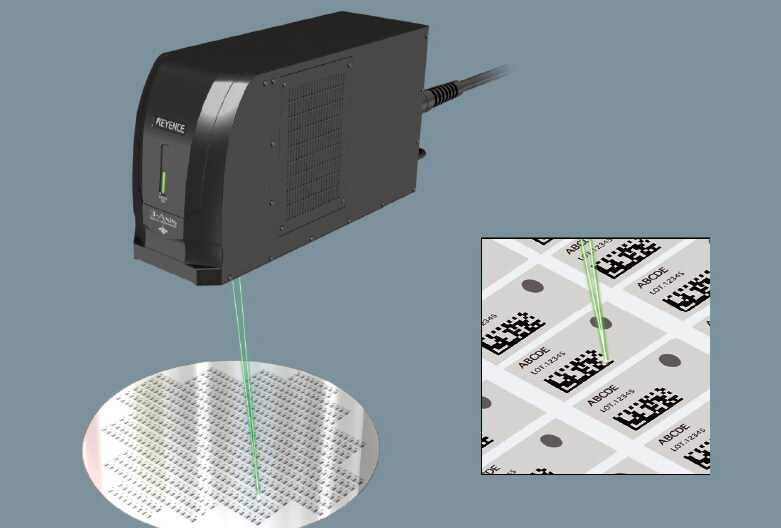
2D code marking on IC chips
Until recently, IC chips were only marked with lot codes. However, a growing need for encoded data has prompted many manufacturers to start using 2D codes.
Micromarking
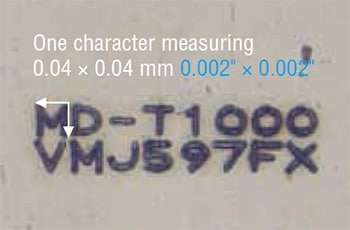
Laser markers have a very small beam spot, making them perfect for applications with a limited marking area. Micromarking - which is typically impossible for most systems - can be accomplished with the right laser. Various marking styles can also be selected, from shallow marking to deep engraving.
Marking on silicon wafer
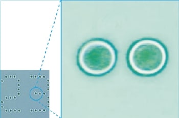
It's vital to keep surface damage to a minimum when marking a finished wafer, otherwise dust and debris can form. That's why UV and green lasers are the optimal wavelengths for these applications.
Marking on LED ceramic package
Due to space limitations, ceramic packages often use 2D codes to contain all the necessary traceability information.
Case2.Deburring
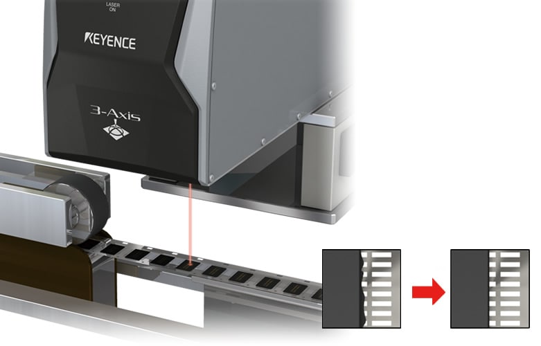
Simultaneous deburring and marking on IC chips
KEYENCE’s 3-Axis laser markers can mark the top surface of IC chips and remove resin burrs as part of the same process.
Since the laser accurately scans only along the edges of the IC, flash burrs over the leads can be removed without causing damage to the inside of the package.
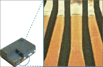
Removing gold plating from connector terminals
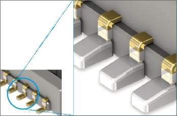
To prevent solder wicking, lasers are used to remove the gold plating from connector terminals.
In the past, masks were used to avoid unnecessary plating. Today, connectors are designed smaller and thinner, and the pitches between the terminals are narrower. Consequently, it has become common practice to apply plating and then remove it with a laser for micron accuracy.
Removing thin-film coating from coil
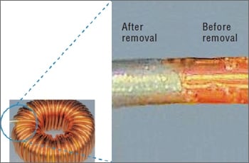
Previously, removers or edged tools were generally used to remove thin-film coating from coils. Now, laser markers have become useful because they require no consumables and ensure stable results.
Resin coating removal
Chemicals are often used to remove resins on defective molds so that the molds can be analyzed. However, chemicals can damage the internal circuit and require multiple man-hours of work. Using a laser marker to remove resin saves running costs and time.
Case3.Patterning
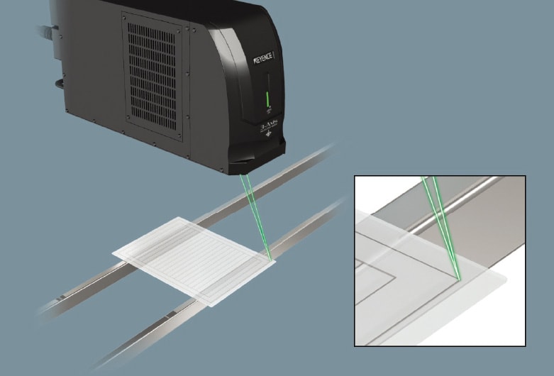
ITO film patterning
Conventional wet etching uses chemicals for ITO film removal and preparation of a patterning mask. However, laser markers don't require chemicals and don't incur any running costs.
Moreover, various patterns can be used by creating layout data through simple programming.
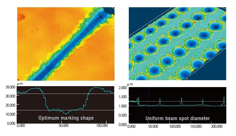
Trimming
Trimming is the process of removing resistance materials, circuit patterns or evaporated films with a laser marker to bring electronic components closer to the desired performance. This technique is indispensable for manufacturing high-quality electronics.
KEYENCE's laser markers feature flexible cutting modes to meet any requirement. Furthermore, you can change the beam spot size and speed during marking to achieve optimal marks.